1
Hardware
Hardware
SEM Input Connectors
About half of the microscopes used for lithography have BNC inputs and do not require any other
input adapter, while on other microscopes, the XY inputs will be in a multiple pin input connector. For
the common models using this arrangement, an adapter will be provided with NPGS to convert from
the multiple pin connector to BNC inputs. When using NPGS v9.0, BNC to SMA cables will be
needed to connect NPGS to the BNC inputs, while NPGS v8.0 uses standard BNC to BNC cables.
When another external system, such as WDS or EDS for X-ray analysis, also needs to control the
beam position, an issue of sharing a single XY input can arise. In this case, either the cable(s) from
NPGS and the other system must be manually swapped, a manual switch must be installed to select
the system to access the XY inputs, or an SEM Input Relay Adapter will be required. The SEM Input
Relay Adapter will allow NPGS and the other system to simultaneously be connected and the
controlling system can be selected by a flip of a switch. For most SEM models, this adapter can be
purchased as an accessory with NPGS.
Note that a few models of SEMs will have multiple inputs for external systems.
In all cases, before doing lithography, the SEM must be switched from the normal internal scan
generator to the external XY control. On most microscopes the external control will be enabled using
a mechanical switch provided with NPGS (most JEOL and Hitachi models) , however, some will be
changed entirely through the SEM software (Philips/FEI XL30 series). A third category is when both a
switch and software is used to enable the external control (LEO/ZEISS models).
Note that in addition to enabling the external control of the XY beam position, in most cases, the
external control of the beam blanker must also be manually enabled. Typically, this is done using a
switch on the control electronics for the blanker.
PCI516 Board (NPGS v9.0 and higher)
Calibrating the PCI516
The PCI516 board has an auto calibration feature that can be run manually using the "Commands Calibrate DACs" option within the NPGS Menu program. This command will reset the board and then
calibrate both the blanking on/off output voltages and the entire 16 bit range for both the x and y DAC
outputs.
Every time the PC is rebooted, the board calibration must be run to ensure that the DAC output
ranges are properly set. Consequently, during the NPGS installation a shortcut in the Windows
Startup directory will be added so that the calibration program will be run every time the PC is
rebooted. The board will be calibrated using the values in the Pg.sys file for the last project used. If
multiple logins will be used under Windows, be sure that the initialization shortcut is the
default for all users. A copy of the initialization shortcut can be found in "\NPGS\Projects", which
can be copied as needed to the Windows "All User" Startup directory.
After the initial calibration, the program will wait for a time (in minutes) listed in
"\NPGS\Projects\Pg_Cal.txt" before calibrating the board a second time. This is to ensure that the PC
has stabilized in temperature after a cold start. During this time, the PC can be used, however,
patterns should not be written before the second calibration has completed.
Configuring the PCI516
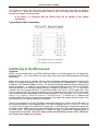
The PCI516 board has only three jumpers that may be manually set by the user. Installing the jumper
"J420" will limit the frequency response of the ADC input on the SMA connector, while removing it will
allow the maximum frequency response. For connections to the image signal from an SEM, the
reduced frequency response is recommended. This jumper is installed when the board is shipped.
SEM Input Connectors • Page 189