1
Chip-Select Module
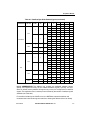
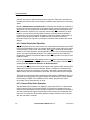
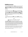
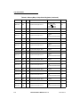
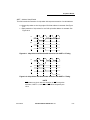
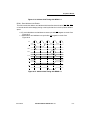
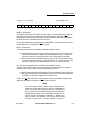
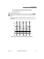
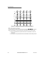
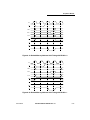
During a write transfers, these outputs indicate which bytes within a long-word transfer are
being selected and which bytes of the data bus will be used for the transfer. WE[0]
controls D[31:24], WE[1] controls D[23:16], WE[2] controls D[15:8] and WE[3] controls
D[7:0]. These signals provide byte data-select signals that are decoded from the SIZx,
A[1:0] signals in addition to the programmed port size and burst capability of the memory
being accessed, as shown in Table 8-1.
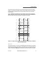
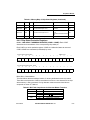
Table 8-1. Data Bus Byte Write-Enable Signals
WE[2]
WE[3]
D[31:24] D[23:16] D[15:8]
D[7:0]
WE[0]
TRANSFER SIZE
PORT SIZE
8-BIT
BYTE
16-BIT
32-BIT
BURST
0/1
0/1
0/1
0
SIZ1
0
0
0
0
SIZ0
A1
WE[1]
A0
0
0
0
1
1
1
0
1
0
1
1
1
1
1
0
0
1
1
1
1
1
0
1
1
1
0
0
0
1
1
1
0
1
1
0
1
1
1
1
0
0
1
1
1
1
1
1
0
1
1
0
0
0
1
1
1
0
1
1
0
1
1
1
1
0
1
1
0
1
1
1
1
1
1
0
0
0
0
1
1
1
0
1
0
1
1
1
1
1
0
0
1
1
1
1
1
0
1
1
1
8-BIT
WORD
1
16-BIT
32-BIT
8-2
0/1
0/1
1
1
1
0
0
0
1
1
1
0
1
0
1
1
1
1
0
0
1
1
1
0
1
1
0
1
1
1
0
0
0
0
1
1
0
1
0
0
0
1
1
0
0
0
0
1
1
1
0
1
1
0
0
0
MCF5206 USERÕS MANUAL Rev 1.0
MOTOROLA