1
2|P a g e
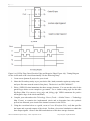
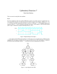
Figure 1(a): D Flip Flop (Gated, Positive Edge and Negative Edge) Figure 1(b): Timing Diagram
for the verification of the circuit functionality. Do the following setup:
1. Create a new Quartus II project for your circuit.
2. Name the file and top entity as per your desire like; latch (remember again top entity name
and your file name must be same in first place). The device is an EP2C20F484C7.
3. Write a VHDL file that instantiates the three storage elements. You can use the code for the
gated D-type below as an example to get started. Use a similar coding style for the other
flip-flops (Hint: You can use rising_edge and falling_edge VHDL statements for positive
and negative edge of the clock transitions).
4. Compile your code and use the Technology Viewer (Tools –> Netlist Viewer –> Technology
Map Viewer) to examine the implemented circuit and to determine how the synthesis
process has allocated your circuit to the internal resources in the FPGA.
5. Using the waveform below as a guide, create a Vector Waveform File (.vwf) that specifies
the inputs and expected outputs of the circuit. Perform a functional simulation to obtain the
three output signals. Observe the different behaviour of the three storage elements.
Advanced FPGA Based System Design - Lab II : Sequential Circuits
Prepared By: Dr. Tayab Din Memon