1
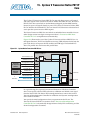
Chapter 12: Stratix V Transceiver Native PHY IP Core
Standard PCS Parameters
12–13
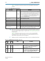
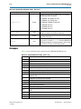
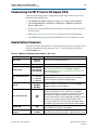
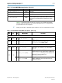
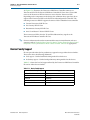
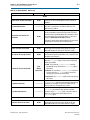
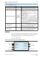
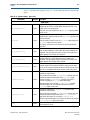
f For more information refer to the Receiver Phase Compensation FIFO and Transmitter
Phase Compensation FIFO sections in Transceiver Architecture in Stratix V Devices.
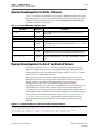
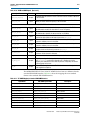
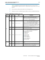
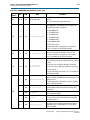
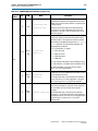
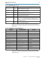
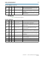
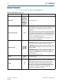
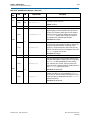
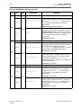
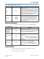
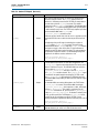
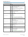
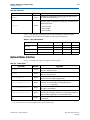
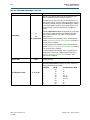
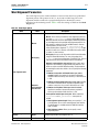
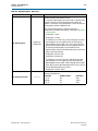
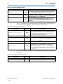
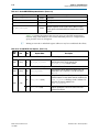
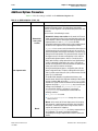
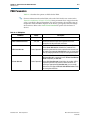
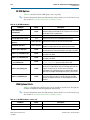
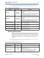
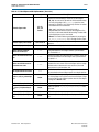
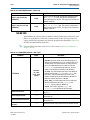
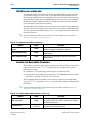
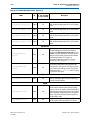
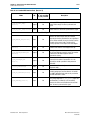
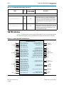
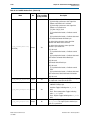
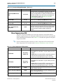
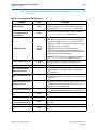
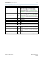
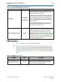
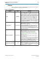
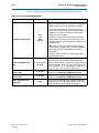
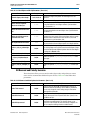
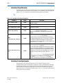
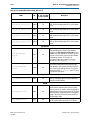
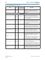
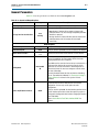
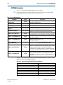
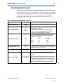
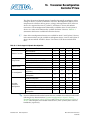
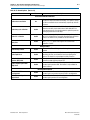
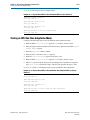
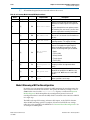
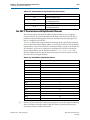
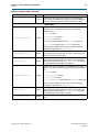
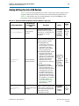
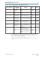
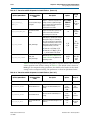
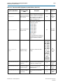
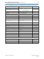
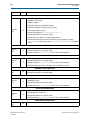
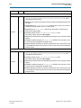
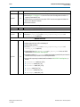
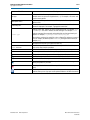
Table 12–12. Phase Compensation FIFO Parameters
Parameter
Range
Description
The following 2 modes are possible:
low_latency
register_fifo
TX FIFO mode
■
low_latency: This mode adds 3–4 cycles of latency to the TX
datapath.
■
register_fifo: In this mode the FIFO is replaced by registers to
reduce the latency through the PCS. Use this mode for
protocols that require deterministic latency, such as CPRI.
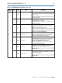
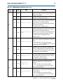
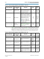
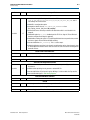
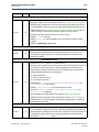
The following 2 modes are possible:
low_latency
register_fifo
RX FIFO mode
■
low_latency: This mode adds 2–3 cycles of latency to the TX
datapath.
■
register_fifo: In this mode the FIFO is replaced by registers to
reduce the latency through the PCS. Use this mode for
protocols that require deterministic latency, such as CPRI.
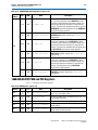
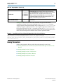
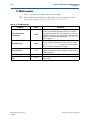
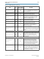
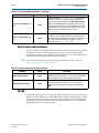
Enable tx_std_pcfifo_full port
On/Off
When you turn this option On, the TX Phase compensation FIFO
outputs a FIFO full status flag.
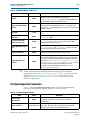
Enable tx_std_pcfifo_empty port
On/Off
When you turn this option On, the TX Phase compensation FIFO
outputs a FIFO empty status flag.
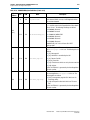
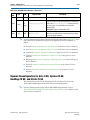
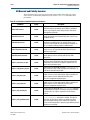
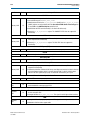
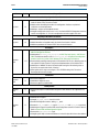
Enable rx_std_pcfifo_full port
On/Off
When you turn this option On, the RX Phase compensation FIFO
outputs a FIFO full status flag.
Enable rx_std_pcfifo_empty port
On/Off
When you turn this option On, the RX Phase compensation FIFO
outputs a FIFO empty status flag.
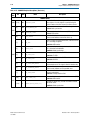
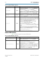
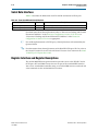
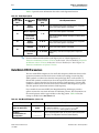
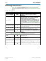
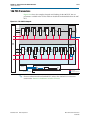
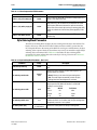
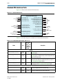
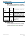
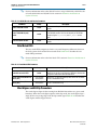
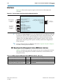
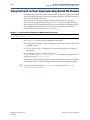
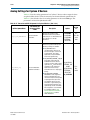
Byte Ordering Block Parameters
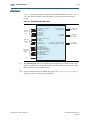
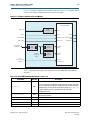
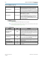
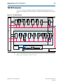
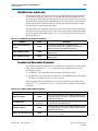
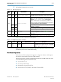
The RX byte ordering block realigns the data coming from the byte deserializer. This
block is necessary when the PCS to FPGA fabric interface width is greater than the
PCS datapath. Because the timing of the RX PCS reset logic is indeterminate, the byte
ordering at the output of the byte deserializer may or may not match the original byte
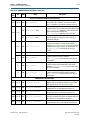
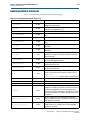
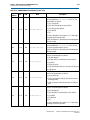
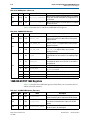
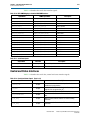
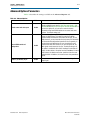
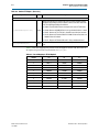
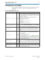
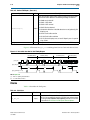
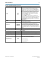
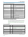
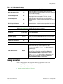
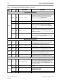
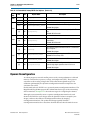
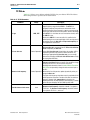
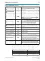
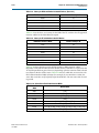
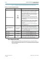
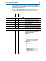
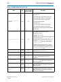
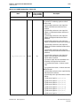
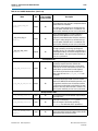
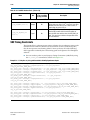
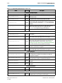
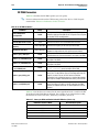
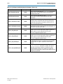
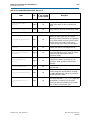
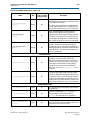
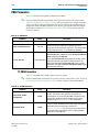
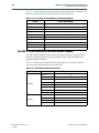
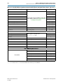
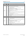
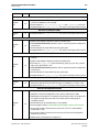
ordering of the transmitted data. Table 12–13 describes the byte ordering block
parameters.
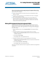
f For more information refer to the Byte Ordering Block section in Transceiver Architecture
in Stratix V Devices.
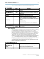
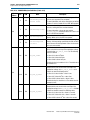
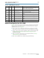
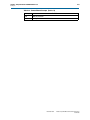
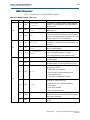
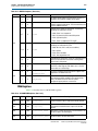
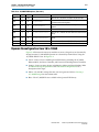
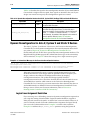
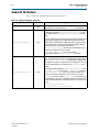
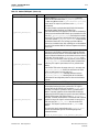
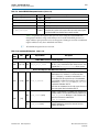
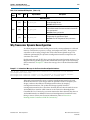
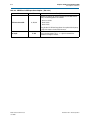
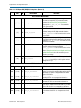
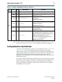
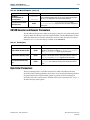
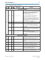
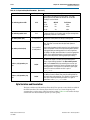
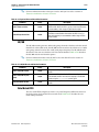
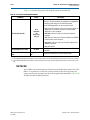
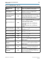
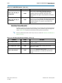
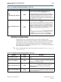
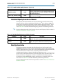
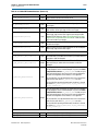
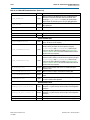
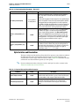
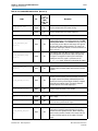
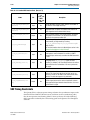
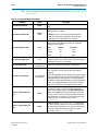
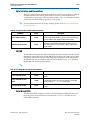
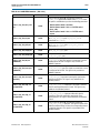
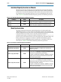
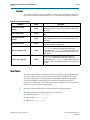
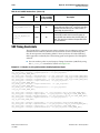
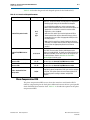
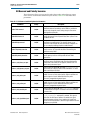
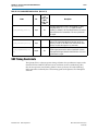
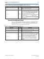
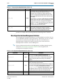
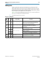
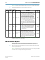
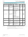
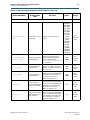
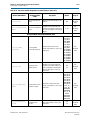
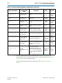
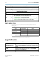
Table 12–13. Byte Ordering Block Parameters (Part 1 of 2)
Parameter
Enable RX byte ordering
Range
Description
On/Off
When you turn this option On, the PCS includes the byte ordering
block.
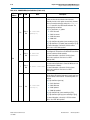
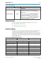
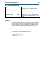
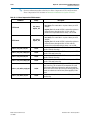
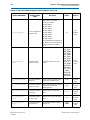
Specifies the control mode for the byte ordering block. The
following modes are available:
Byte ordering control mode
November 2012
Altera Corporation
manual
auto
■
Manual: Allows you to control the byte ordering block
■
Auto: The word aligner automatically controls the byte
ordering block once word alignment is achieved.
Altera Transceiver PHY IP Core
User Guide