1
Electrical Specifications
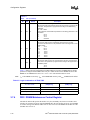
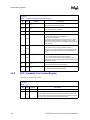
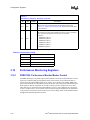
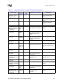
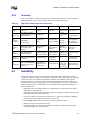
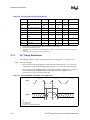
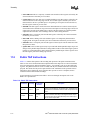
Table 9-30. CMOS 3.3 V AC Parametersa,b (Continued)
Symbol
Min
Max
Unit
SRf
Output Slew Rate Fall
1
4
V/ns
SRr
Output Slew Rate Rise
1
4
V/ns
a.
b.
9.9
Parameter
Notes
Supply voltage at 1.5V ±5% tolerance.
Clock delay is in reference to the 200 MHz clock.
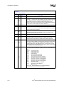
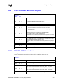
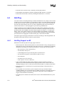
Clock Signal Groups
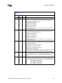
Table 9-31. Clock Signal Groups
Signal Group
Signals
LVHSTL Differential Inputs
BUSCLK, BUSCLK#
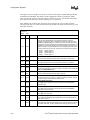
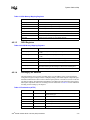
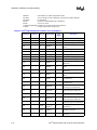
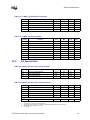
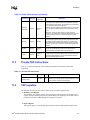
Table 9-32. LVHSTL Clock DC Parameters
Symbol
9.9.1
Parameter
Min
Typ
Max
Unit
VIH
Input High Voltage
0.78
1.3
V
VIL
Input Low Voltage
–0.3
0.5
V
VX
Input Crossover Voltage
0.55
0.85
V
CCLK
Input Capacitance
1.0
11.5
pF
AC Specification
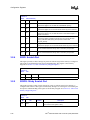
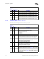
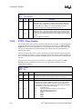
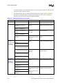
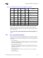
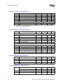
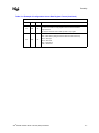
Table 9-33. LVHSTL Differential Clock AC Specification
Symbol
Parameter
Min
Typ
Max
Unit
Notes
ns
a
200
MHz
a,b
100
ps
a,c
Tperiod
BUSCLK Period
fBCLK
BUSCLK Frequency
Tjitter
BUSCLK Input Jitter
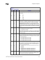
Thigh
BUSCLK High Time
2.25
2.5
2.75
ns
a,d
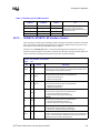
Tlow
BUSCLK Low Time
2.25
2.5
2.75
ns
a,d
Trise
BUSCLK Rise Time
333
500
667
ps
a
Tfall
BUSCLK Fall Time
333
500
667
ps
a
VPP
Minimum Input Swing
mV
a,e
a.
b.
c.
d.
e.
5.0
200
600
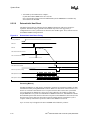
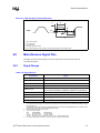
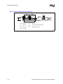
See Figure 9-4.
Measured on cross point of rising edge of BUSCLK and falling edge of BUSCLK#. Long term jitter is defined as peak-to-peak
variation measured by accumulating a large number of clock cycles and recording peak-to-peak jitter.
Long term jitter is defined as peak-to-peak variation measured by accumulating a large number of clock cycles and recording
peak-to-peak jitter.
Measured on cross point of rising edge of BUSCLK and falling edge of BUSCLK#.
VPPmin is defined as the minimum input differential voltage which will cause no increase in the clock receiver timing.
Intel® E8870 Scalable Node Controller (SNC) Datasheet
9-15