1
Application Note 1501
Power Supply
Audio Outputs
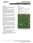
The DC power supply connected at banana jacks J1
(VCC) and J2 (GND) provides power to the evaluation
board. The IC requires a +2.7V to +5.0V DC power
supply for proper operation. The power supply should be
capable of delivering 100µA of current.
The evaluation board has a standard headphone jack
(J11) connected to the COM- and COM+ pins. A
headphone with a 3.5mm audio jack can be plugged into
the evaluation board.
Logic Control
The state of the ISL54409 and ISL54410 device is
determined by the voltage at the IN pin and the CTRL
pin. When the JP1 three pin jumper is in the 1-2 position,
access to the IN pin is through the BNC connector J3.
When the jumper is in the 2-3 position, access to the IN
pin is through switch S1. When the JP2 three pin jumper
is in the 2-3 position, access to the CTRL pin is through
the BNC connector J8. When the jumper is in the 1-2
position, access to the CTRL pin is through switch S2.
The IN and CTRL pins are 1.8V logic compatible which
allows for control via a standard µcontroller.
Logic “0” (LOW) when ≤ 0.5V or floating
Logic “1” (HIGH) when ≥ 1.4V
Note: The evaluation board has a 1MΩ pull-down resistor
from the IN pin to ground and CTRL pin to ground. In
addition, the ISL54409 and ISL54410 IC have an internal
4MΩ pull-down resistor on the IN and CTRL logic pins. If
the user wishes to remove the 1MΩ resistors on the
board simply depopulate R2 for the CTRL pin and R3 for
the IN pin.
If IN is LOW and CTRL is HIGH the part will be in the
Audio mode. The switches will be ON and can pass audio
signals from the LIN/RIN to COM-/COM+. If IN is driven
HIGH and CTRL = X (don’t care) the part will be in the
USB mode. The switches will be turned OFF, providing
excellent signal isolation from LIN/RIN to COM-/COM+.
For the ISL54409 if IN is logic “0”and CTRL is logic “0”
the part will be in the Low Power mode. In Low Power
mode both switches are OFF and the part will draw less
than 10nA typically.
For the ISL54410 if IN is logic “0”and CTRL is logic “0”
the part will be in the Audio Click and Pop mode. In Audio
Click and Pop mode both switches are OFF and the
LIN/RIN pins will have a 40Ω shunt path to ground.
*Note that in a typical application the USB and audio
connections use a common connector. This evaluation
board has separate connectors for USB and audio for
simplicity in evaluating the performance of USB and
audio signals. However, for optimal USB 2.0 HS
performance, the headphone jack can be disconnected
from the COM-/COM+ path. This can be done by
depopulating resistors R6 and R7 on the evaluation
board.
USB Connections
A type A USB receptacle (J4) and a type B USB
receptacle (J5) is located on the left side of the board.
The type B receptacle should be connected using a
standard USB cable to the upstream USB host controller
which is usually a PC computer or hub. A USB device can
be plugged directly into this receptacle. When this
connection is made and the IN logic control is driven
HIGH, the ISL54409, ISL54410 device will go into USB
mode. The switches will be turned OFF and the USB Host
and USB device can communicate.
Note: Before operating in the USB mode, the
headphones must be removed from the headphone
speaker jack. This will prevent the audio load from
interfering with USB signal transmission. The main
purpose of the ISL54409, ISL54410 IC is to allow the use
of a common USB and Audio Headphone Connector in
Personal Media Players and other portable battery
powered equipment. Either a headphone will be in the
common connector to play music or a USB cable from a
computer will be in the common connector to transmit
digital data.
TABLE 1. EVALUATION BOARD COMPONENT
DEFINITIONS
DESIGNATOR
DESCRIPTION
U1
ISL54409IRUZ or ISL54410IRUZ IC
J1
VCC Banana Jack Connection
Audio Inputs
J2
GND Banana Jack Connection
The evaluation board has two audio inputs, LIN (J9) and
RIN (J10) using BNC connectors on the right side of the
evaluation board. Over a signal range of -1V to +1V
(0.707VRMS) these switches have an extremely low
ON-resistance variation. The rON of the switch is typically
less than 3Ω. They can pass ground referenced audio
signals with very low distortion (<0.04% THD+N) when
delivering 4mW into a 32Ω headphone speaker load. A
signal range above 0.707VRMS is acceptable but THD+N
performance will degrade.
J3
IN Logic Control; BNC Connector
2
J4, J5
Standard USB Connectors
J8
CTRL Logic Control; BNC Connector
J9
LIN BNC Connector
J10
RIN BNC Connector
S1
IN Logic Control; Toggle Switch
S2
CTRL Logic Control; Toggle Switch
AN1501.0
October 8, 2009