1
MOTOROLA
CPU CYCLE
CPU CYCLE
S0
S2
S4
S0
S2
S4
CPU CYCLE
DMA WRITE
S0
S2
S4
S0
S2
S4
DMA WRITE
S0
S2
CLKOUT
A31–A0
FC3–FC0
SIZ1-SIZ0
AS
MC68340 USER’S MANUAL
DS
R/W
D15–D0
DSACKx
DREQx
DONEx
(INPUT)
DACKx
DONEx
(OUTPUT)
NOTE:
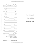
1. DREQx must be active for two consecutive clocks for a DMA request to be recognized.
2. To cause another DMA transfer, DREQx is asserted after DACKx is asserted and before DACKx is negated.
3. DACKx and DONEx (DMA control signals) are asserted in the destination (write) DMA cycle.
6-11
Figure 6-8. Single-Address Write Timing (Cycle Steal)
S4