1
FUNCTIONAL DESCRIPTION
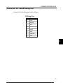
Table 3-1 depicts the memory map for the ipEngine-1:
ipEngine-1 Memory Map
Address Range
Description
0000.0000 – 00FF.FFFF
16 MB DRAM
FC00.0000 – FC7F.FFFF
8MB FPGA Space
FE00.0000 – FE3F.FFFF
4 MB FLASH
FF00.0000 – FF00.3FFF
MPC823 On-Chip Registers
FF01.0000 – FF01.0000
FPGA Config Register
FF02.0000 – FF02.0000
Clock Synth Reg
3
Flash and DRAM Memory
The on-board 2M (1Mx16), BootBlock FLASH memory provides storage for the
operating system as well as OEM application and data.
The lowest two memory blocks are the "boot" blocks that are factory
programmed with the boot monitor software, board serial number, and Ethernet
MAC (hardware address). These blocks are locked and cannot be erased or
reprogrammed. This is to ensure there is always some way to reload the board in
case all the other flash block is erased or have been loaded with faulty code.
Blocks 2 and 3 are used for parameter storage. These parameters, such as the IP
address for the board and others, are used by the boot monitor software. See
Chapter 5 for a complete description of the parameters used by the boot monitor.
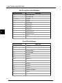
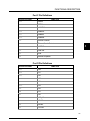
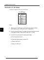
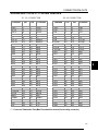
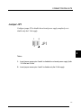
The following four tables specify the connection between the MPC823 multifunction ports A-D and specific ipEngine signals/functions:
3-3