1
1
3
1 . 5
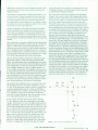
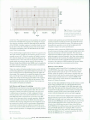
DR_REF(V)
3
. 5
4
4 . 5
V¡n p-p differential (mV)
5.5
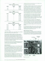
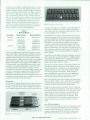
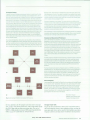
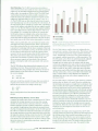
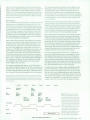
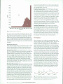
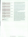
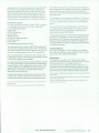
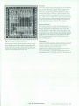
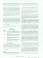
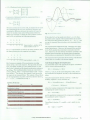
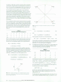
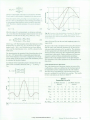
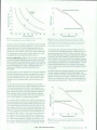
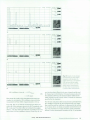
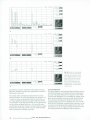
Fig. 10. LOS threshold as a function of DR_REF.
Fig. 11. BER as a function of data input amplitude.
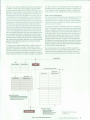
HDMP-1526 transceiver is a 10-bit, 1062.5-Mbaud transceiver
designed for this Fibre Channel arbitrated loop (FC-AL)
market It is a descendant of the HDMP-1512/HDMP-1514
20-bit, 1062.5/531.25-Mbaud transmitter/receiver chipset.
The Fibre Channel chipset has many functions not needed in
the FC-AL transceiver chip, such as optical interface blocks.
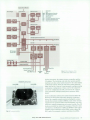
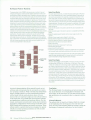
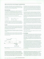
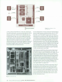
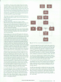
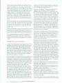
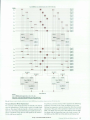
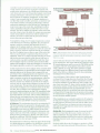
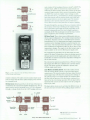
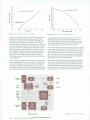
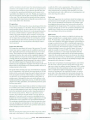
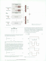
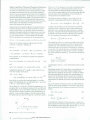
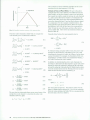
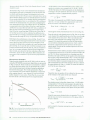
Fig. 12 shows the block diagram of the transceiver. The re
duction in functions and the change to a 10-bit bus allowed
the integration of both transmitter and receiver functions
onto a single die, using a proprietary HP device array. The
transceiver uses a 10-bit parallel interface running at
106.25 Mbaud instead of a 20-bit parallel interface running
at53.125Mbaud.
the ping-pong selector. The loopback ports were also de
leted because an internal connection is possible with a
single-chip design. This leaves just one high-speed output
port and one-high speed input port. Other timing changes
were implemented to fit specific customer needs.
Deletions on the transmitter side include the ac laser driver
and its supporting dc bias circuitry and the comma genera
tor function. Deletions on the receiver side include the power-on/reset circuitry, the loss-of-signal circuitry, and the
cable equalizer function. Deleted functions common to both
the transmitter and receiver include the speed selector and
Isolating the two independent phase-locked loops within a
3.54-mm-by-3.54-mm area presented the biggest challenge
during the layout of the chip. The transmitter and receiver
phase-locked loops are placed at opposite corners to mini
mize cross talk. Various portions of the chip are isolated by
using separate power supplies and bandgap references.
In the single-chip design, select inputs and clocks are shared
between the transmitter and receiver. This lowers the power
requirements, reduces the number of pins, and makes pos
sible a smaller chip size if a custom layout is done at a later
date. The transceiver, with its 1.8-watt total power dissipa
tion (compared to 3 watts for the chipset), is packaged in a
single 64-pin 14-by-14-mm quad flat pack.
Data Byte
±DOUT
TX[0-9]
LOOPEN
TXCAPO
TXCAP1
Transmitter
Phase-locked
Loop and
Clock Generator
±DOUT
REFCLK —
-LCKREF —
Receiver
Phase-Locked
Loop and
Clock Recovery
RXCAPO —
RXCAP1 —
RBCO
RBC1
Internal
Receive
Clocks
Data Byte
RX[0-9]
BYTSYNC ENBYTSYNC
66 February 1996 Hewlett-Packard Journal
© Copr. 1949-1998 Hewlett-Packard Co.
Fig. 12. Transceiver block diagram.