1
External Clock Operation
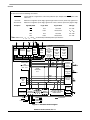
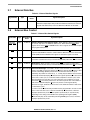
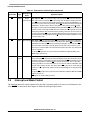
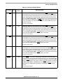
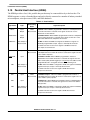
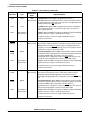
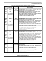
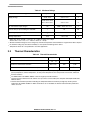
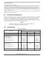
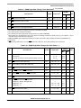
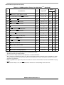
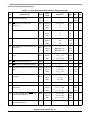
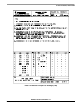
Table 3-4 Internal Clocks (continued)
Expression1, 2
Characteristics
Symbol
Min
Typ
Max
TC
—
2 × ETC
—
ICYC
—
TC
—
Internal clock cycle time with PLL disabled
Instruction cycle time
1
DF = Division Factor
Ef = External frequency
ETC = External clock cycle
MF = Multiplication Factor
PDF = Predivision Factor
TC = internal clock cycle
2
Refer to the DSP56300 Family Manual for a detailed discussion of the PLL.
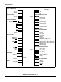
3.7
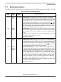
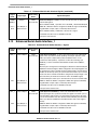
External Clock Operation
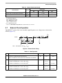
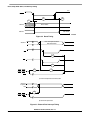
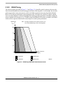
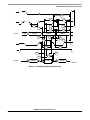
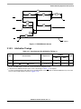
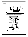
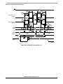
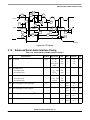
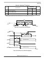
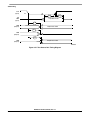
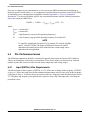
The DSP56367 system clock is an externally supplied square wave voltage source connected to
EXTAL(Figure 3-1).
VIHC
Midpoint
EXTAL
VILC
ETH
ETL
2
4
3
ETC
Note: The midpoint is 0.5 (VIHC + VILC).
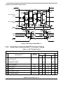
Figure 3-1 External Clock Timing
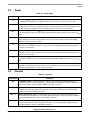
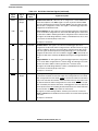
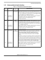
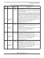
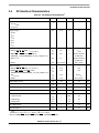
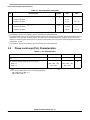
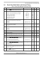
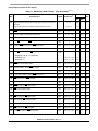
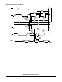
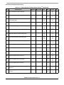
Table 3-5 Clock Operation
No.
1
Characteristics
Symbol
Min
Max
Ef
2.0 ns
150.0
cycle3)
3.11 ns
∞
3)
2.83 ns
157.0 µs
3
3.11 ns
∞
3
2.83 ns
157.0 µs
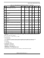
Frequency of EXTAL (EXTAL Pin Frequency)
The rise and fall time of this external clock should be 2 ns maximum.
2
EXTAL input high1, 2
ETH
• With PLL disabled (46.7%–53.3% duty
• With PLL enabled (42.5%–57.5% duty cycle
3
EXTAL input low1, 2
ETL
• With PLL disabled (46.7%–53.3% duty cycle )
• With PLL enabled (42.5%–57.5% duty cycle )
DSP56367 Technical Data, Rev. 2.1
Freescale Semiconductor
3-5