1
In both of these encoding schemes, clock bits are written at the start of their respective bit cells and data bits at the
center of their bit cells.
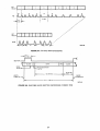
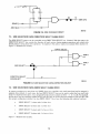
The timing of the read signals, READ DATA, SEPARATED DATA, and SEPARATED CLOCK are shown in
figure 1-6 (FM encoding).
In the standard SA810/860, data separation of FM data is performed by the drive electronics. Data bits are
presented to the controller on the SEP DATA line and clock bits are presented on the SEP CLOCK line. In systems
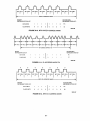
using MFM encoding, data separation is performed outside the drive. In such cases, the READ DATA line carries
both clock bits and data bits. Separation of MFM encoded read data should be controlled by a phase-locked loop
circuit.
For additional information regarding the use of MFM encoding, refer to paragraph 6.2.
1.4.9 Write Operation
Writing data to the SA810/860 is accomplished by:
a.
Activating DRIVE SELECT line.
b.
Selecting head.
c.
Activating WRITE GATE line.
d.
Pulsing WRITE DATA line with data to be written.
e.
Head current switching.
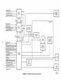
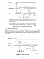
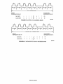
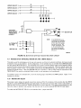
The timing relationships required to initiate a write data sequence are shown in figure 1-8. These timing specifications are required in order to guarantee that the read/write head position has stabilized prior to writing.
Write data encoding can be FM or MFM. If MFM is used, the write data should be precompensated to counter the
effects of bit shift. The amount and direction of compensation required for any given bit in the data strea'm depends
on the pattern it forms with nearby bits.
For more details regarding data encoding and formatting for SA810/860 drives, refer to Section VI.
DC POWER
DRIVE
SELECT
I--
90 ms MIN
-----I
I
I
1-
'65 ms MIN1
STEP
SIDE SELECT
(SA860 ONLY)
-I----.U
r-9~~S~--1~ I !--------11
16 ms MIN'
100
I(S MIN
r-i
I_--------------~
WRITE GATE
WRITE DATA
r
-I
i-------..U
* Or
4
'SMIN
U
u
when TRUE READY comes active
39216·07·A
FIGURE 1·8. WRITE INITIATE TIMING
1-9