1
AT83SND2CMP3
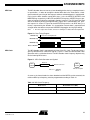
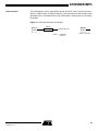
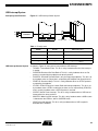
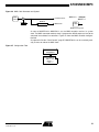
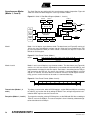
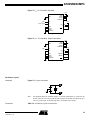
Fi gure 7) . Value of the filter components ar e detailed in the Section “ DC
Characteristics”.
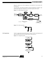
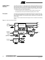
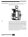
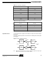
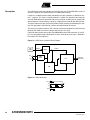
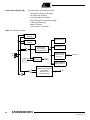
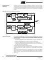
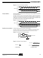
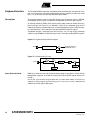
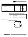
The VCO block is the Voltage Controlled Oscillator controlled by the voltage Vref produced by the charge pump. It generates a square wave signal: the PLL clock.
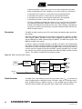
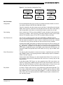
Figure 6. PLL Block Diagram and Symbol
PFILT
PLLCON.1
PLLEN
N divider
OSC
CLOCK
Up
N6:0
PFLD
CHP
Vref
VCO
Down
PLOCK
PLL
Clock
R divider
PLLCON.0
R9:0
PLL
CLOCK
OSCclk × ( R + 1 )
PLLclk = ----------------------------------------------N+1
PLL Clock Symbol
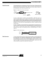
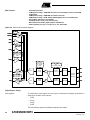
Figure 7. PLL Filter Connection
FILT
R
C2
C1
VSS
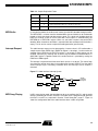
PLL Programming
VSS
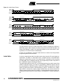
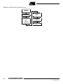
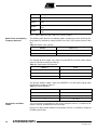
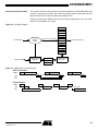
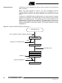
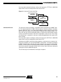
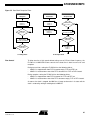
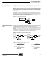
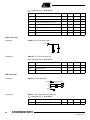
The PLL is programmed using the flow shown in Figure 8. The PLL clock frequency will
depend on MP3 decoder clock and audio interface clock frequencies.
Figure 8. PLL Programming Flow
PLL
Programming
Configure Dividers
N6:0 = xxxxxxb
R9:0 = xxxxxxxxxxb
Enable PLL
PLLRES = 0
PLLEN = 1
PLL Locked?
PLOCK = 1?
11
7524D–MP3–07/07