1
Silicon Updates
www.ti.com
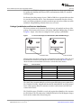
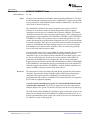
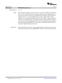
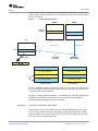
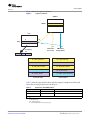
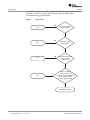
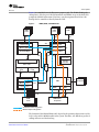
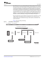
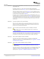
Figure 3 shows the sequence of events.
Figure 3
Sequence of Events
UMAPx
SRAM
L1D
t2
t1
Dirty
t3
t0
CPU Read
(L2 Cache)
Corruption
t3’
DMA Write
(Snoop Write)
t4
t0: CPU Allocate
t0: CPU Allocate
t1: Victim Start
t1: Victim Start
t2: Allocation Data
t2: Allocation Data
t3: DMA Write (SNPW)
t3: Victim Done
t4: Victim Done
t4: DMA Write (SNPW)
Correct Order
Incorrect Order
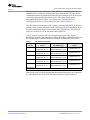
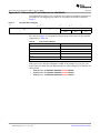
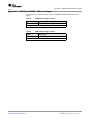
Table 7 shows the expected data values after this sequence completes and the actual
values that are now present because of this issue.
.
Table 7
Expected vs. Actual Data Values1
Buffer
Expected
Actual
Buffer A
A’’’
B’’
Buffer B
B’’
B
End of Table 7
1. Key:
A, B = Original Data
A’ = CPU-written data
A’’, B’’ = DMA-written data
A’’’ = CPU-and-DMA-written data, properly merged
SPRZ293A—November 2009
Submit Documentation Feedback
TMS320C6457
Fixed-Point Digital Signal Processor Silicon Errata
Silicon Revisions 1.0, 1.1, 1.2, 1.3, 1.4
25
.