1
The way in which the LSI counters are used depends
on the number of cycles which must be counted. For
very short delays, the output "A/N" may be preset
high by setting the output of the last LSI counter,
U206 pin 17, low. In this case, the LSI counters are
not used in the delay cycle.
KICKPULSE
OTA's (Operational Transconductance
Amplifiers) are used throughout the system to
precharge capacitors when the delay cycle is
complete. The maximum steady state bias
current to these devices is only a few milliamps,
so, in order to rapidly recharge these capacitors,
a "kick pulse" isused to boost the current by
several milliamps at the start of the reset cycle.
This "kick pulse" is generated by differentiating
the 800 ns GATE pulse, amplifying it with an
OTA, and buffering with a Darlington pair.
For delays which require 1 to 32767 ticks of the HC
counter in the delay, the output of the LSI counter
which is connected to the or-gate is set low,
allowing the last LSI counter to count the HC ticks.
The last LSI counter's output goes low on the
terminal count.
For delays which require more than 32767 ticks of
the HC counter, the LSI counter which is clocked by
the inverted output of the HC counter, is
programmed to divide by 32768. The next LSI
counter's output will go low after 1 to 65535 ticks of
the first LSI counter thus gating the HC counter's
output to the last LSI counter. The last LSI counter's
output goes low after 1 to 65,535 counts.
THE T0 DIGITAL DELAY
The T0 output is similar to the A, B, C, and D
output, except the delay cannot be adjusted.
When a trigger is received, 4/4 of U104 gates
the 80 MHz clock to U201T. The first rising
edge of the 80 MHz clock sets Q-bar of 1/2
U201T, which clocks 1/2 of U103, asserting the
T0-CNT to indicate the completion of the digital
count for the T0 delay. The analog delay portion
of the T0 delay is identical to the analog delays
of the other channels.
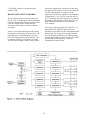
The output from the HC counter (A/64) and the
inverted output from the last LSI counter (A/N) are
passed to the bottom PCB for synchronization to the
80MHz reference oscillator. The ECL flip-flop, 1/2
U202A, is clocked by A/64; if the D-input (A/N) is
high (indicating that the LSI count is complete) then
the Q-bar output of the flip-flop will go low. This
eliminates the jitter of the LSI counter, as the ECL
output is synchronous with the HC counter's
transition. The final synchronization is done by the
2/2 of U202A. This flip flop is clocked by the ECL
output of the synchronous two-bit ECL counter
(20MHz toggle rate). Its output will change states
synchronously with the first clock input after the Qbar output of the 1/2 of U202A goes low. The
outputs of 2/2 of U202A going low signal the end of
the digital count. The channel will stop counting and
the analog delay for the channel will be started.
CHANNEL A's DIGITAL DELAY
The digital delays are essentially identical for all
of the channels; the references in this
description will be to channel A.
When a trigger is received, an 80MHz reference
is provided by the ECL OR Gate, U106, to the
two-bit ECL counter, U201A. The high bit of
this counter is shifted to TTL levels by 1/4 of
U203 and passed to the "top" PCB. This bit,
"A/4", is used as the clock input to the 4-bit
binary counter U304 (a 74HC191). The high bit
of the HC counter, "A/64", is used as a clock to
the uPD8253 LSI counters. The maximum clock
frequency to the HC counter is 20MHz and the
maximum clock frequency to the LSI counters is
1.25MHz.
ANALOG DELAYS
The analog delays for each output, T0, A, B, C and
D, are essentially the same. Circuit references to
channel A will be used in this description.
The quad 1:2 multiplexer, U309, passes the A
inputs to the Y outputs during the count cycle.
During the 820ns reset cycle, this multiplexer
sends the LOAD pulse (at the B input) to the
LSI counters' clock inputs to reload the counters
for the next timing cycle.
The analog delays are controlled by charging a
capacitor (C309A) with a constant current source
(Q304A). The constant current source, and so the
delay calibration, is controlled by D/A output
(A_CAL) from the processor. When the digital
27