1
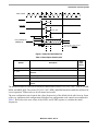
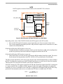
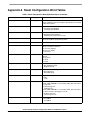
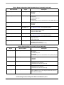
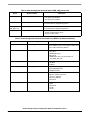
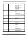
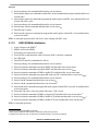
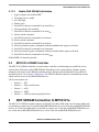
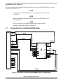
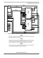
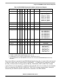
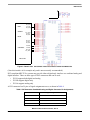
Usage of the DRAM Controller Command Registers
Bit
31
30
29
28
27
26
25
24
23
22
21
20
19
18
17
16
CMD
REQ
0
CS
RAS
CAS
WEB
BA2
BA1
BA0
R
W
Bit
15
14
13
12
11
10
9
8
7
6
5
4
3
2
1
0
CKE
disable
A14
A13
A12
A11
A10
A9
A8
A7
A6
A5
A4
A3
A2
A1
A0
R
W
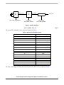
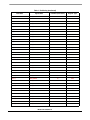
Figure 19. Command Register
Table 9. Field Descriptions of the Command Register
Field
Description
CMDREQ
If this bit is set then the command defined by bits [23:0] will be sent to the DDR SDRAM.
CS
Controls the output of the MPC5121e CS pin.
RAS
Controls the output of the MPC5121e RAS pin.
CAS
Controls the output of the MPC5121e CAS pin.
WEB
Controls the output of the MPC5121e WEB pin.
BA2
Controls the output of the MPC5121e BA2 pin.
BA1
Controls the output of the MPC5121e BA1 pin.
BA0
Controls the output of the MPC5121e BA0 pin.
CKE disable
Disables the CKE line at the same time as sending the command.
A14
Controls the output of the MPC5121e A14 pin.
A13
Controls the output of the MPC5121e A13 pin.
A12
Controls the output of the MPC5121e A12 pin.
A11
Controls the output of the MPC5121e A11 pin.
A10
Controls the output of the MPC5121e A10 pin.
A9
Controls the output of the MPC5121e A9 pin.
A8
Controls the output of the MPC5121e A8 pin.
A7
Controls the output of the MPC5121e A7 pin.
A6
Controls the output of the MPC5121e A6 pin.
A5
Controls the output of the MPC5121e A5 pin.
A4
Controls the output of the MPC5121e A4 pin.
A3
Controls the output of the MPC5121e A3 pin.
A2
Controls the output of the MPC5121e A2 pin.
A1
Controls the output of the MPC5121e A1 pin.
A0
Controls the output of the MPC5121e A0 pin.
MPC5121e DRAM Controller, Rev. 2
82
Freescale Semiconductor