1
Page 26
Epson Research and Development
Vancouver Design Center
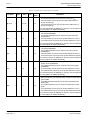
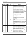
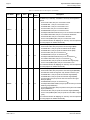
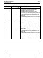
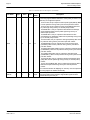
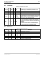
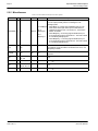
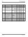
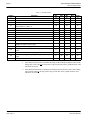
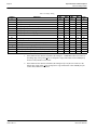
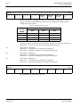
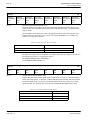
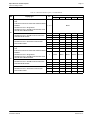
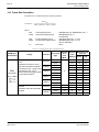
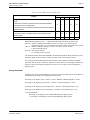
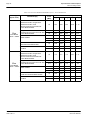
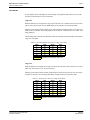
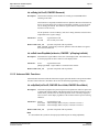
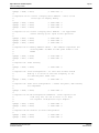
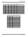
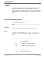
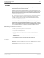
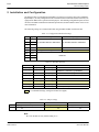
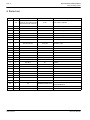
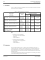
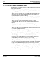
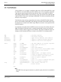
Table 5-1: Host Interface Pin Descriptions (Continued)
Pin Name
Type
Pin #
Cell
RESET#
State
Description
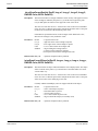
This pin inputs the system bus clock. It is possible to apply a 2x clock
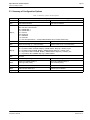
and divide it by 2 internally - see MD12 in Summary of Configuration
Options.
BUSCLK
I
13
C
Hi-Z
•
•
•
•
•
•
•
•
•
For SH-3/SH-4 Bus, this pin is connected to CKIO.
For MC68K Bus 1, this pin is connected to CLK.
For MC68K Bus 2, this pin is connected to CLK.
For Generic Bus, this pin is connected to BCLK.
For MIPS/ISA Bus, this pin is connected to CLK.
For Philips PR31500/31700 Bus, this pin is connected to DCLKOUT.
For Toshiba TX3912 Bus, this pin is connected to DCLKOUT.
For PowerPC Bus, this pin is connected to CLKOUT.
For PC Card (PCMCIA) Bus, this pin is connected to CLKI.
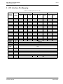
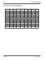
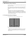
See “Host Bus Interface Pin Mapping” for summary. See the respective
AC Timing diagram for detailed functionality.
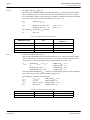
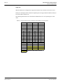
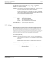
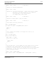
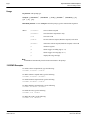
This is a multi-purpose pin:
BS#
I
6
CS
Hi-Z
•
•
•
•
•
•
•
•
•
For SH-3/SH-4 Bus, this pin inputs the bus start signal (BS#).
For MC68K Bus 1, this pin inputs the address strobe (AS#).
For MC68K Bus 2, this pin inputs the address strobe (AS#).
For Generic Bus, this pin is connected to V DD.
For MIPS/ISA Bus, this pin is connected to VDD.
For Philips PR31500/31700 Bus, this pin is connected to VDD.
For Toshiba TX3912 Bus, this pin is connected to VDD.
For PowerPC Bus, this pin inputs the Transfer Start signal (TS#).
For PC Card (PCMCIA) Bus, this pin is connected to VDD.
See “Host Bus Interface Pin Mapping” for summary. See the respective
AC Timing diagram for detailed functionality.
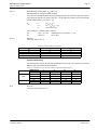
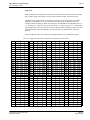
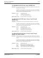
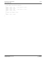
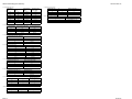
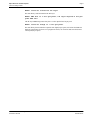
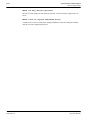
This is a multi-purpose pin:
RD/WR#
I
10
CS
Hi-Z
• For SH-3/SH-4 Bus, this pin inputs the read write signal (RD/WR#).
The SED1355 needs this signal for early decode of the bus cycle.
• For MC68K Bus 1, this pin inputs the read write signal (R/W#).
• For MC68K Bus 2, this pin inputs the read write signal (R/W#).
• For Generic Bus, this pin inputs the read command for the upper
data byte (RD1#).
• For MIPS/ISA Bus, this pin is connected to VDD.
• For Philips PR31500/31700 Bus, this pin inputs the even byte access
enable signal (/CARDxCSL).
• For Toshiba TX3912 Bus, this pin inputs the even byte access enable
signal (CARDxCSL*).
• For PowerPC Bus, this pin inputs the read write signal (RD/WR#).
• For PC Card (PCMCIA) Bus, this pin inputs the card enable 1 signal
(-CE1).
See “Host Bus Interface Pin Mapping” for summary. See the respective
AC Timing diagram for detailed functionality.
SED1355
X23A-A-001-11
Hardware Functional Specification
Issue Date: 99/05/18