1
Freescale Semiconductor, Inc.
Signals
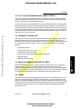
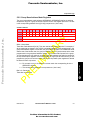
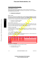
2.1.7 Interrupt Control Pins
AR
IN
PM5-PM2/IRQ1, IRQ2, IRQ3, IRQ6
These pins can be programmed to either parallel I/O PM2-PM5 or interrupt input. When they
function as interrupt inputs, they can be programmed to be edge or level triggered with either
high or low polarity. IRQ6 generates a level 6 interrupt. IRQ3, IRQ2, and IRQ1 generate
level 3, 2 and 1 interrupts respectively.
2.1.8 Chip Select Pins
CSA0—BOOT CHIP-SELECT
CSA0 is the default chip-select after reset. It is set to 6 wait states and decodes all address
ranges except internal register address space. It can be reprogrammed during the boot
sequence to another address range and a different number of wait states.
IM
SIGNAL DESCRIPTIONS
Y
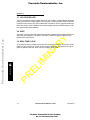
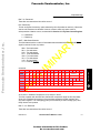
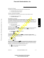
PM6/PENIRQ—PEN INTERRUPT INPUT AND GENERAL-PURPOSE I/O
Users can program this pin as a general-purpose I/O PM6 or pen-interrupt input. When
programmed as a pen-interrupt signal, this pin accepts an active low, level-triggered
interrupt from the pen input device for a “pen-down” action.
PR
EL
2
Freescale Semiconductor, Inc...
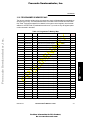
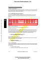
PD0-PD7/KB0-KB7/INT0-INT7—KEYBOARD AND GENERAL-PURPOSE INTERRUPT
LINES
Users can program these signals as interrupt inputs or parallel I/O ports. For an interrupt port
application, INT0-INT7 can be configured to perform keyboard interrupt functions. Keyboard
interrupt pins KB0-KB7 are pulled high internally and connected to the rows of the keyboard
matrix with the column driven low. When any one key of the row lines is pressed, an interrupt
is generated to signal to the CPU to scan the keys. This feature, together with the pen
interrupt, contributes a significant portion of the power management activities.
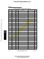
PE7-PE1/CSB3-CSB0, CSA3-CSA1—CHIP-SELECT GROUP A AND B
These pins comprise the remainder of the Group A and Group B chip-selects and are
individually programmable. Pins that are not needed as chip-selects can be programmed as
general-purpose I/Os. By default after reset, CSB3 is disabled and functions as a generalpurpose input.
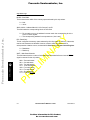
PJ7-PJ0/CSD3-CSD0/CSC3-CSC0—CHIP-SELECT GROUP C AND D
These pins comprise the Group C and Group D chip-selects and are individually
programmable. Pins that are not needed as chip-selects can be programmed as generalpurpose I/Os.
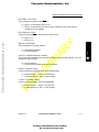
2.1.9 PCMCIA 1.0 PINS
PC6/WE—WRITE ENABLE, PC6
This pin can be programmed as either PC6 parallel I/O or a write-enable signal for the
PCMCIA 1.0 card interface. The MC68328 processor drives the active-low WE signal to
indicate a memory-write transfer to the PCMCIA 1.0 card. When programmed as I/O, it
serves as PC6.
2-6
MC68328 USER’S MANUAL 11/6/97
For More Information On This Product,
Go to: www.freescale.com
MOTOROLA