1
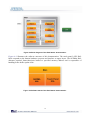
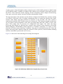
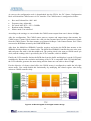
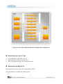
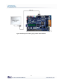
As soon as the configuration code is downloaded into the FPGA, the I2C Sensor Configuration block will initial the CMOS sensor via I2C interface. The CMOS sensor is configured as follow: Row and Column Size: 800 * 600 Exposure time: Adjustable Pix clock: MCLK*2 = 25*2 = 50MHz Readout modes: Binning Mirror mode: Line mirrored According to the settings, we can calculate the CMOS sensor output frame rate is about 44.4 fps. After the configuration, The CMOS sensor starts to capture and output image data streams, the CMOS sensor Capture block extracts the valid pix data streams based on the synchronous signals from the CMOS sensor. The data streams are generated in Bayer Color Pattern format. So it‟s then converted to RGB data streams by the RAW2RGB block. After that, the Multi-Port SDRAM Controller acquires and writes the RGB data streams to the SDRAM which performs as a frame buffer. The Multi-Port SDRAM Controller has two write ports and read ports also with 16-bit data width each. The writing clock is the same as CMOS sensor pix clock, and the reading clock is provided by the LCD Controller, which is 40MHz. Finally, the LCD controller fetches the RGB data from the buffer and displays it on the LCD panel continuously. Because the resolution and timing of the LCD is compatible with SVGA@800*600, the LCD controller generates the same timing and the frame rate can achieve about 25 fps. For the objective of a better visual effect, the CMOS sensor is configured to enable the left right mirror mode. User could disable this functionality by modifying the related register value being written to CMOS controller chip. Figure 4-12 Block diagram of the digital camera design 29