1
5 . Physical Size and Pad Layout
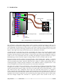
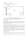
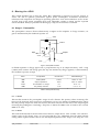
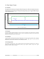
The overall dimensions of the APV6 chip are shown in Figure 2 below.
Four groups of
32 input pads
1
INP<127>
VSS
APV6
GND
VDD
1
13
INP<0>
37
Bias monitor pads
Back-end pads
Figure 2: APV6 overall dimensions (dimensions in microns)
The design will be fabricated using the standard Harris AVLSI-RA process flow. The wafers will be
of 4 inch type and 19mils (approx. 500um) thick. A table showing the precise co-ordinates of t h e
centre of each pad may be obtained from RAL, please request it if required.
5.1 Analogue inputs
The 128 analogue inputs are grouped into four sections of 32. Each section is separated by larger power
supply pads. These power connections supply the preamplifier stages (where most of the APV6 power
is used) and must be bonded to supplies close to the chip. Use the shortest bond length and multiple
bonds if possible (to minimise inductance).
Note: The reason for powering the chip in this way is so that the power losses in the APV6
routing, and the area wasted in large power buses is minimised.
Each group of inputs is arranged in two staggered rows, each rows pads are spaced at 86um. The inner
row is offset 43um clockwise (viewed from the centre of the APV6). Thus the effective bond pitch
within each group is 43 um. Each pad is 100um long and 60um wide (the passivation opening is about
3um smaller than this). The pads are labelled from <0> to <127>. The Inp<0> is on the lower left of
the first group and Inp<127> is at the top right of the top section.
The analogue inputs all have small protection diodes to VSS and VDD. These are not intended to
meet standard levels of protection but should prevent damage during assembly if reasonable antistatic measures are taken. For them to work effectively the VDD GND and VSS pads should be
bonded first and grounded to the assembly machine.
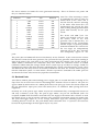
5.2 Bias monitor pads
These are intended for test purposes only. They enable a direct measurement of the bias voltages and
currents set in the bias generator. The first test systems should permit bonding to these points to allow
apv6_manual.doc
Version: Draft
7
16/10/96