1
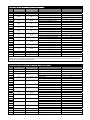
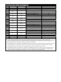
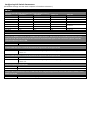
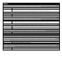
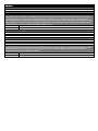
Pinouts (TIA‐449 with adapter cable information) Pin FOM‐1091 (DCE) Direction FOM‐1090 (DTE) Direction TIA‐449 Configuration DB‐37 Pin 1 Chassis Ground 1 7 Signal Ground 19, 20, 37 2 Send Data A (SD) (V.11) 4 Out In 14 Send Data B (SD\) (V.11) 22 3 Receive Data A (RD) (V.11) 6 In Out 16 Receive Data B (RD\) (V.11) 24 4 Request To Send A (RTS) (V.11) 7 Out In 19 Request To Send B (RTS\) (V.11) 25 5 Clear To Send A (CTS) (V.11) 9 In Out 13 Clear To Send B (CTS\) (V.11) 27 20 Terminal Ready A (TR) (V.11) 12 Out In 23 Terminal Ready B (TR\) (V.11) 30 6 Data Set Ready A (DSR) (V.11) 11 In Out 22 Data Set Ready B (DSR\) (V.11) 29 24 Terminal Timing A (TT) (V.11) 17 Out In 11 Terminal Timing B (TT\) (V.11) 35 8 Receiver Ready A (RR) (V.11) 13 In Out 10 Receiver Ready B (RR\) (V.11) 31 15 Send Timing A (ST) (V.11) 5 In Out 12 Send Timing B (ST\) (V.11) 23 17 Receive Timing A (RT) (V.11) 8 In Out 9 Receive Timing B (RT\) (V.11) 26 18 Out In Local Loopback (LL) (V.10) 10 25 In Out Test Mode (TM) (V.10) 18 21 Out In Remote Loopback (RL) (V.10) 14 Note: For best signal performance do not tie pin 20 (Receive Common), pin 37 (Send Common), or pin 19 (Signal Ground) together at the DB‐37 connector. Bring all three pins back on individual conductors to pin 7 of the DB‐25 and tie them together there. Pinouts (TIA‐232; TIA‐574 with adapter cable information) Pin 1 7 2 14 3 16 4 19 5 13 20 23 6 22 24 11 8 10 15 12 17 9 18 25 21 FOM‐1091 (DCE) Direction Out ‐ In ‐ Out ‐ In ‐ Out ‐ In In Out ‐ In ‐ In ‐ In ‐ Out In Out FOM‐1090 (DTE) Direction In ‐ Out ‐ In ‐ Out ‐ In ‐ Out Out In ‐ Out ‐ Out ‐ Out ‐ In Out In TIA‐232 Configuration Chassis Ground Signal Ground TD (V.28) ‐ RD (V.28) ‐ RTS/RS (V.28) ‐ CTS/CS (V.28) ‐ DTR/TR (V.28) ‐ DSR/DM (V.28) RI/IC (V.28) TT (V.28) ‐ DCD/RR (V.28) ‐ ST (V.28) ‐ RT (V.11) ‐ LL (V.28) TM (V.28) RL (V.28) TIA‐574 DB‐9 Pin ‐ 5 3 ‐ 2 ‐ 7 ‐ 8 ‐ 4 ‐ 6 9 ‐ ‐ 1 ‐ ‐ ‐ ‐ ‐ ‐ ‐ ‐