1
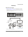
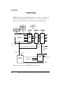
Auxiliary PWM Generation Unit
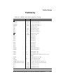
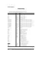
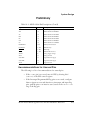
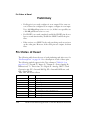
Preliminary
Operation Features
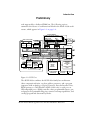
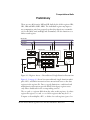
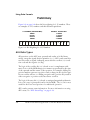
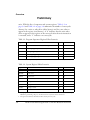
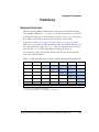
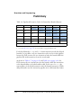
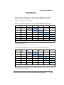
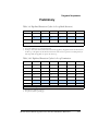
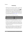
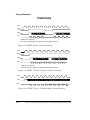
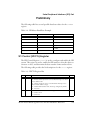
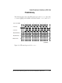
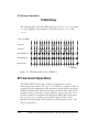
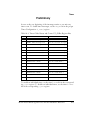
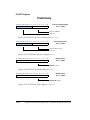
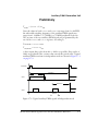
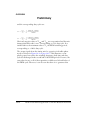
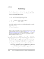
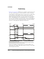
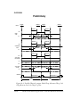
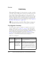
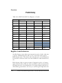
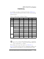
In both operating modes, the resolution of the auxiliary PWM system is
16-bit only at the minimum switching frequency (AUXTM0 = AUXTM1 =
65535 in independent mode, AUXTM0 = 65535 in offset mode). Obviously
as the switching frequency is increased the resolution is reduced.
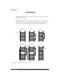
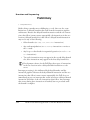
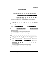
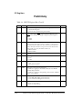
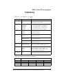
Values written to the auxiliary PWM registers are double buffered and
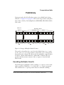
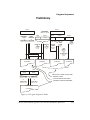
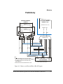
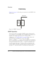
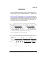
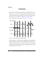
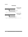
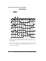
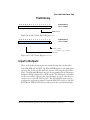
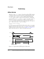
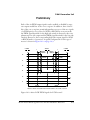
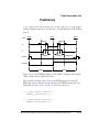
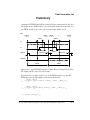
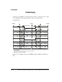
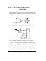
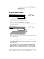
cause updates in the auxiliary PWM system at period boundaries. In independent mode, the AUXTM0 and AUXCH0 values will be applied at the
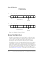
beginning of the next Auxiliary PWM period, defined as the rising edge of
AUX0. Each auxiliary PWM output behaves independently in the same
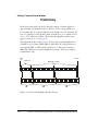
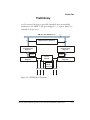
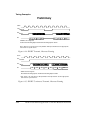
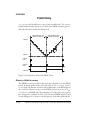
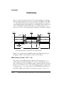
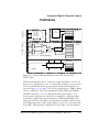
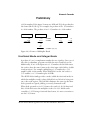
update manner. In offset mode, AUXTM0, AUXCH0, and AUXTM1 values will be
applied at the beginning of the next AUX0 period, defined as the rising edge
of AUX0. The AUXCH1 value is updated when the AUX1 output begins its
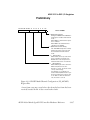
period after the AUXTM1 defined offset. By default, following power on or a
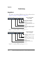
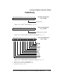
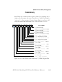
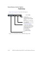
reset, bit 4 of the AUXCTRL register is cleared so that offset mode is enabled.
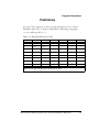
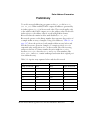
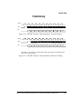
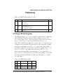
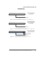
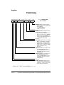
In addition, the registers AUXTM0 and AUXTM1 default to 0xFFFF, corresponding to minimum switching frequency and zero offset. In addition,
the on-time registers AUXCH0 and AUXCH1 default to 0x0000. The state of
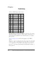
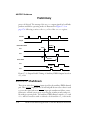
the two auxiliary PWM output signals, AUX0 and AUX1, may be read in the
AUXSTAT2 register and can be used for software observation of the PWM
ADSP-2199x Mixed Signal DSP Controller Hardware Reference
17-5