1
SPBT2632C2A
7.5
Hardware design
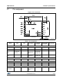
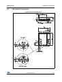
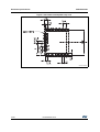
PCB layout guidelines
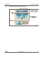
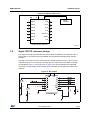
Figure 9. PCB layout guidelines
VXUURXQGLQJ
$0Y
7.6
Reset circuit
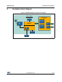
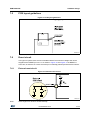
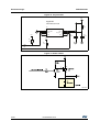
Two types of system reset circuits are detailed below.The maximum voltage that can be
supplied to the RESET pin is 2.5 V. As shown in Figure 10 and Figure 11 the RESET is
active low, in absence of a reset circuit the pin is internally pulled up and therefore inactive.
7.6.1
External reset circuit
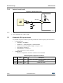
Figure 10. External reset circuit
5(6(7
$0Y
Note:
RPU ranges from 30 kΩ to 50 kΩ internally.
DocID022833 Rev 6
21/30
30