1
ComDeC
LSPM2
4.3.3 EEPROM control
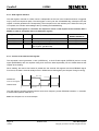
Since the memory has a serial interface, the data, addresses and also the commands for switching over to
the various operating modes must be transferred to it serially. The specified module awaits a 2-bit Op code
after a start bit (log. "1") and then a 6-bit address, i.e. 9 bits, in order to switch to the corresponding mode.
Data is read or written only after this.
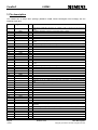
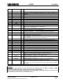
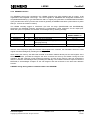
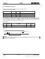
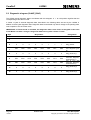
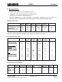
The following Op codes are generated:
Command
Start bit/Opcode
READ WORD
ERASE/WRITE-ENABLE
WRITE WORD
110
100
101
Address (binary)
000000 bzw. 000001
110000
000000
An erase cycle is not required since the memory overwrites the corresponding word when writing.
The word with address 000 000Bin is generally addressed in the EEPROM, but an Erase/Write-Enable cycle is
executed before each write access operation since the module is generally in Erase/Write-Disable mode after
the power is restored.
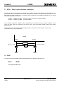
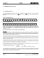
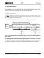
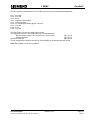
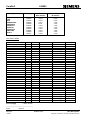
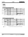
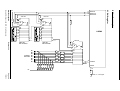
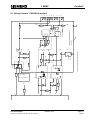
The integrated controller of the LSPM2 generates a clock (INTERCLK) and a Chip-Select signal (INTERCS)
with the corresponding timing and clocks the control bits and data out sequentially when writing or into an
internal shift register when reading.
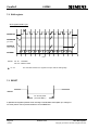
min. 4µs
INTERCLK
Clock for EEPROM
internal clock
min. 2µs
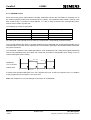
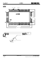
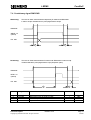
A read access operation takes 200 µs for one complete read cycle. A write cycle requires 100 µs, in addition
to the programming time of approx. 10 ms per word.
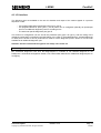
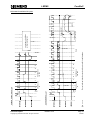
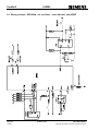
Note: See Chapter 8 for a circuit example of connection of an EEPROM.
Page 16
10/2002
Release V2.0
User Description
Copyright (C) Siemens AG 2002. All rights reserved.