1
GR8BIT knowledge base article #KB0009
•
•
•
•
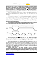
CLKHI, the high frequency clock signal, generated by the CPU board’s
crystal;
CLKLO, the standard VDP output frequency, for GR8BIT it is 3.58MHz;
IORQ as the trigger for braking. Note that you can combine different
triggering signals using simple logic (e.g. AND elements, if all signals are
active negative). The only requirement is that this composite triggering
input signal is active low;
Three (ACTx) as other optional triggering signals for braking (of your
choice);
and one output signal, CPUCLK, which clocks CPU (and some other circuits if you
choose so – read on).
Here’s a description of the functions of the logic elements on the schematic:
• IC5A: 4-input NAND logic gate, which outputs high level in case any of
input lines go low – e.g. IORQ on pin 1 goes active. You can connect 3
more low-active signals (e.g. slot select signals);
• IC5B: 4-input NAND logic gate, which suspends clocking impulses to the
counter IC4A;
• IC4A/IC4B: these are counters which count clock cycles supplied to
them, and present number of cycles counted on their outputs in binary
representation. These two 4-bit binary counter elements are daisy-chained
to form one 8-bit binary counter. This daisy-chained structure outputs a
positive-edge impulse BRAKE . Minimal number of cycles counted (if you
choose to connect pin 3 of IC5A to the pin 3 of IC4A, is 0 or 1/2 (depends
on the phase of its input clock at pin 1), maximal number of cycles
counted (if you choose to connect pin BRAKE to the pin 8 of IC4B) is 128
or 128.5 its input clock cycles at the pin 1 of IC4A. The selection of the
number of cycles which activates signal BRAKE can only be a power of 2
– 0 (20, pin 3), 2 (21, pin 4), 4 (22, pin 5), 8 (23, pin 6), 16 (24, pin 11), 32
(25, pin 10), 64 (26, pin 9) and 128 (27, pin 8). It does not look like a
great set of options, but it is enough to flat-tune to the acceptable level of
system reliability. You can add another counter in the same way as IC4,
and increase number of cycles counted above 7th power of 2. Moreover,
you have a flexibility to choose the IC4A clock source, which is used to
calculate number of cycles – either CLKHI, or CLKLO – and it is clear that
with CLKHI you can set number of cycles versus brake time more
precisely, however maximal absolute interval of time for IC4 to generate
strobe/triggering signal will decrease appropriately.
• IC3A/IC3B/IC6 is a reliable clock switching circuit, developed by the
Alwin Henseler (NL), and published and implemented in his Super-Turbo
device back in 1998.
© 2012 Eugeny Brychkov
http://www.gr8bit.ru
Page 5 / 17
Status: Released