1
STM32 F4 ADC GUI
STM32 F4 ADC GUI
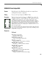
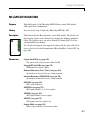
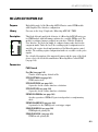
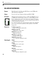
Purpose
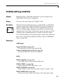
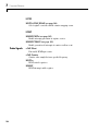
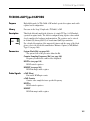
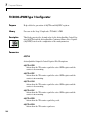
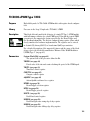
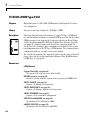
High fidelity model of STM32 F4 ADC module with Graphical User Interface
configuration.
Library
Processor in the Loop / Peripherals / STM32 F4 / ADC
Description
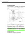
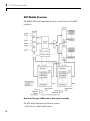
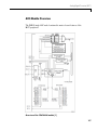
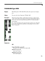
This block models the STM F4 ADC module. With the Graphical User Interface, the block can simply be configured using combo boxes in the component
mask. Under the hood, the resulting register configuration is forwarded to the
register based implementation of the STM F4 ADC module. The resulting register configuration further is accessible via the probe signals.
For a detailed description of the supported features and the usage of the block
please refer to the detailed documentation “Analog Digital Converter (ADC)”
(on page 126).
Parameters
ADC General
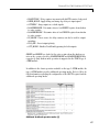
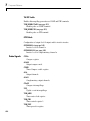
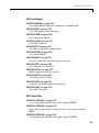
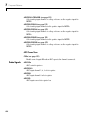
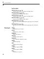
PCLK2 [Hz] (see page 128)
The clock used as as the adc time base in Hz.
ADC_CCR.ADCPRE (see page 128)
Register cell defining a clock prescaler.
Reference[LO,HI] (see page 128)
Specification of the reference voltage in mask.
ADC_CR1.RES (see page 128)
Defines ADC resolution.
ADC_CR1.DISCNUM (see page 129)
Defines regular channels converted in discontinuous mode.
ADC_CR1.JDISCEN (see page 129)
Enables discontinuous mode for injected channels.
ADC_CR1.DISCEN (see page 129)
Enables/disables discontinuous mode for regular channels.
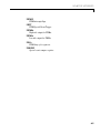
ADC_CR1.JAUTO (see page 129)
Enables/disables automatic injected group conversion.
203