1
8XC196NP SPECIFICATION UPDATE
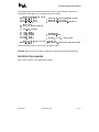
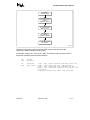
The following code excerpt adds instructions to force P3.0 low while the chip-select
configuration takes place, then reconfigure the pin as CS0#.
GENERATE A ØFAKEÙ #3 ACTIVE
ANDB P?DIR?E ./4 CONFIGURE 0 AS COMPLEMENTARY OUTPUT
ANDB P?REG?E ./4 CONFIGURE 0 TO DRIVE ANDB P?MODE?E ./4
CONFIGURE 0 AS GENERALPURPOSE )/
SET UP #3
TMP IS A SCRATCH REGISTER
ST ZERO?REG ADDRMSK
LD
ST
ST
LDB
STB
TMP
TMP
TMP
TMP
TMP
EH
ADDRCOM
ADDRMSK
CH
BUSCON
ADDRESS %H
RANGE %&H
DEMUXED BITS WAIT STATES
RESTORE #3 CONTROL OVER THE 0#3 PIN
ORB P?MODE?E CONFIGURE 0 AS SPECIAL FUNCTION #3
This same method can be used for any chip-select output.
STATUS: Refer to Summary Table of Changes to determine the affected stepping(s).
SPECIFICATION CHANGES
None for this revision of this specification update.
272838-002
September, 1996
9 of 17