1
B.1.2
CMOS Level I/O
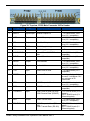
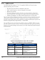
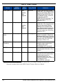
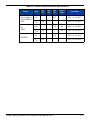
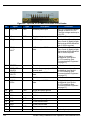
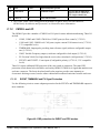
The OEM628 provides a number of 2.7V (3.3V-compatible) CMOS-level I/O pins for status
indication and timing. These I/O include:
•
PPS: Pulse-Per-Second (software configurable to other rates)
•
VARF: Variable Frequency (a software-configurable clock output)
•
ERROR: Error indication
•
PV: Position Valid (used to indicate when the receiver has calculated a valid position)
•
EVENT1 and EVENT2: Event inputs (active high by default with configurable polarity)
•
USERIO1 and USERIO2: User GPIO (available through NovAtel’s UserApp API)
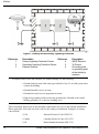
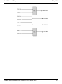
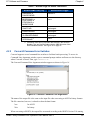
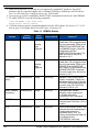
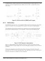
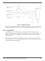
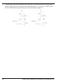
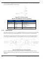
These I/O require additional ESD protection if they are routed to connectors. Some users may require
additional drive strength on the PPS signal. The figure below shows a suitable buffer that may be
used. R103 in the schematic may be used to limit the drive strength of the PPS output if required. This
buffer has a propagation delay of approximately 5 – 6 nanoseconds.
The same ESD protection circuit shown below should be used on any OEM628 CMOS-level signal
that will be routed to an enclosure connector. The ferrite bead and small-value capacitor provide some
immunity to electrostatic discharge events, but also serve to reduce radiated and conducted emissions
from the enclosure.
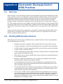
Figure 32: ESD protection for EVENT and PPS strobes
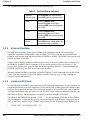
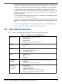
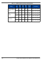
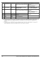
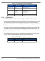
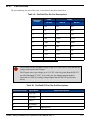
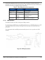
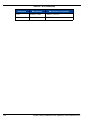
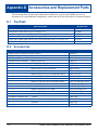
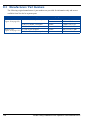
Table 15: Bill of Materials (critical components)
Designator
108
Manufacturer
Manufacturer part number
FFB100, FB101
TDK
MMZ1005B800C
U100
Texas Instruments
SN74LVC1G86DCK
U101
Semtech
Bourns
OnSemi
LC03-6.TBT
CDNBS08-PLC03-6
LC03-6R2G
C101, C102
various
(22 pF 5% 50V COG 0603)
OEM6 Family Installation and Operation User Manual Rev 4