1
CubeSuite+ V2.01.00
CHAPTER 4 ASSEMBLY LANGUAGE SPECIFICATIONS
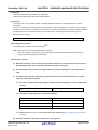
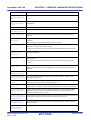
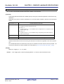
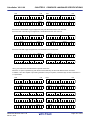
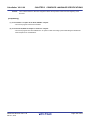
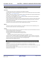
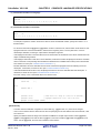
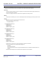
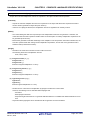
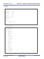
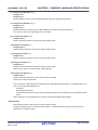
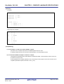
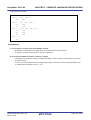
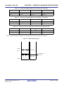
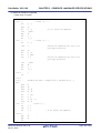
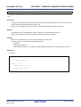
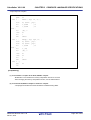
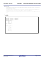
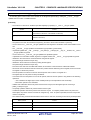
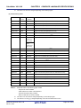
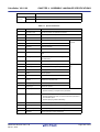
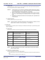
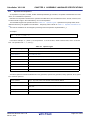
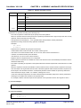
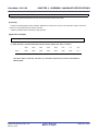
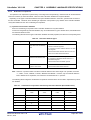
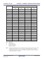
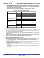
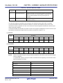
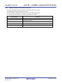
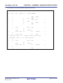
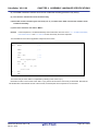
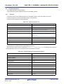
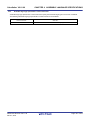
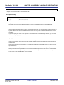
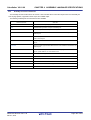
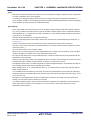
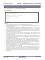
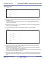
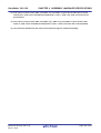
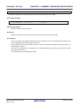
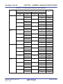
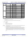
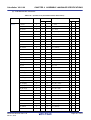
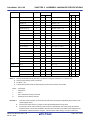
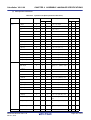
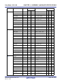
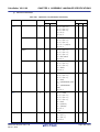
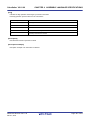
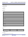
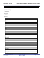
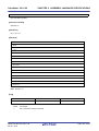
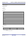
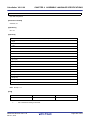
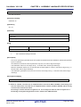
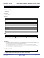
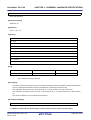
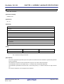
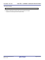
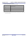
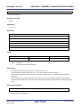
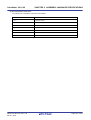
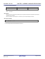
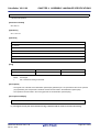
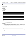
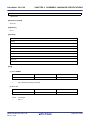
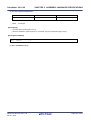
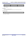
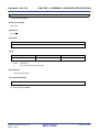
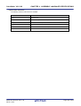
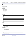
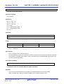
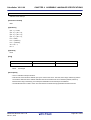
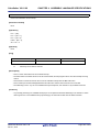
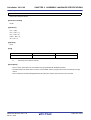
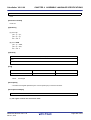
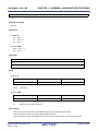
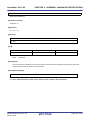
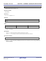
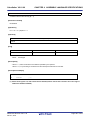
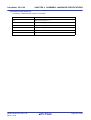
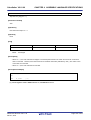
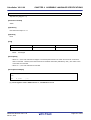
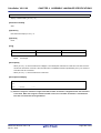
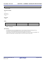
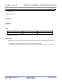
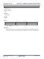
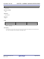
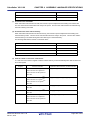
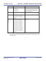
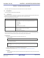
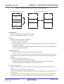
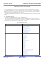
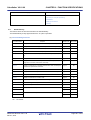
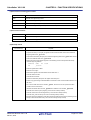
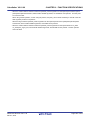
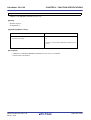
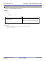
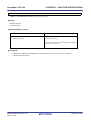
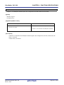
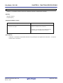
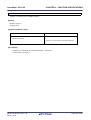
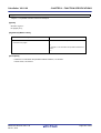
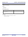
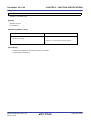
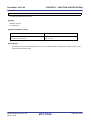
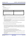
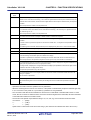
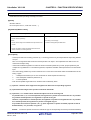
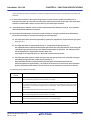
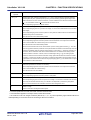
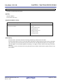
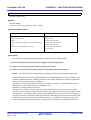
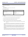
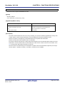
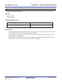
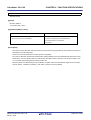
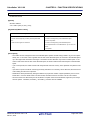
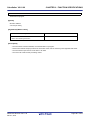
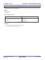
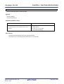
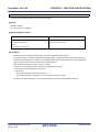
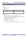
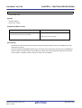
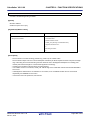
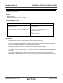
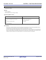
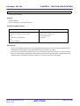
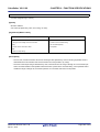
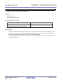
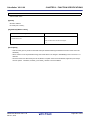
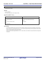
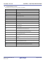
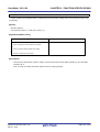
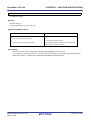
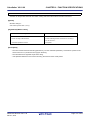
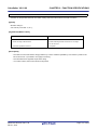
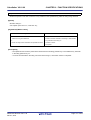
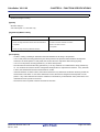
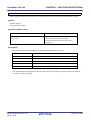
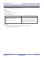
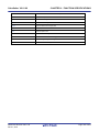
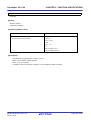
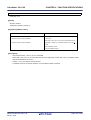
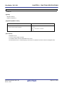
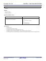
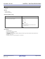
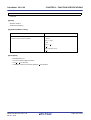
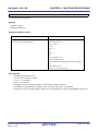
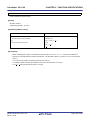
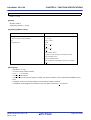
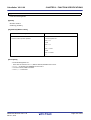
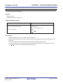
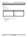
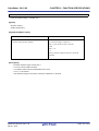
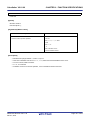
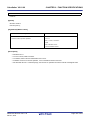
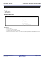
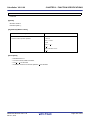
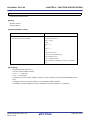
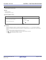
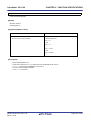
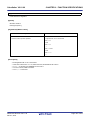
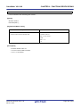
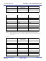
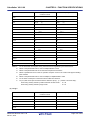
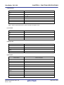
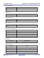
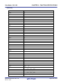
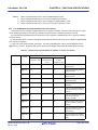
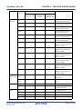
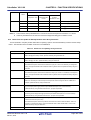
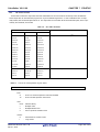
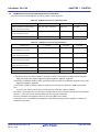
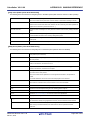
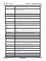
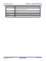
(g) Shift instructions
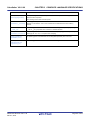
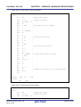
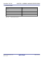
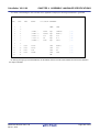
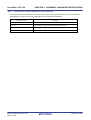
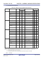
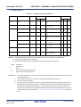
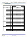
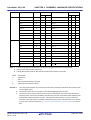
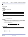
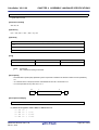
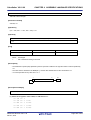
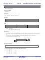
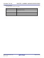
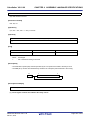
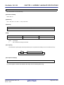
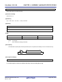
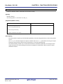
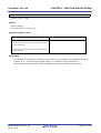
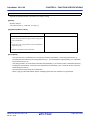
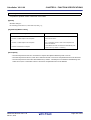
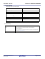
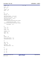
Table 4-37. Operation List (Shift Instructions)
Mnemonic
SHR
Operand
A, cnt
Byte
Clock
Note 1
Note 2
1
-
2
FlagNote 3
Operation
Z
AC
(CY <- A0, Am-1 <- Am, A7 <- 0)
CY
x
x cnt
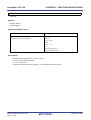
SHRW
AX, cnt
2
1
-
(CY <- AX0, AXm-1 <- AXm,
x
AX15 <- 0) x cnt
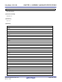
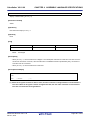
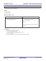
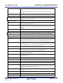
SHL
A, cnt
2
1
-
(CY <- A7, Am <- Am-1, A0 <- 0)
x
x cnt
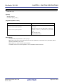
B, cnt
2
1
-
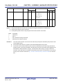
(CY <- B7, Bm <- Bm-1, B0 <- 0)
x
x cnt
C, cnt
2
1
-
(CY <- C7, Cm <- Cm-1, C0 <- 0)
x
x cnt
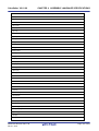
SHLW
AX, cnt
2
1
-
(CY <- AX15, AXm <- AXm-1,
x
AX0 <- 0) x cnt
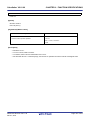
BC, cnt
2
1
-
(CY <- BC15, BCm <- BCm-1,
x
BC0 <- 0) x cnt
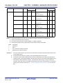
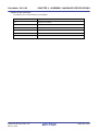
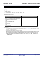
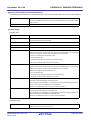
SAR
A, cnt
2
1
-
(CY <- A0, Am-1 <- Am, A 7 <- A7)
x
xcnt
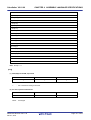
SARW
AX, cnt
2
1
-
(CY <- AX0, AXm-1 <- AXm,
x
AX15 <- AX15) x cnt
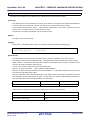
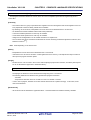
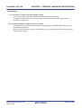
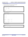
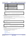
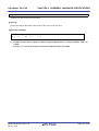
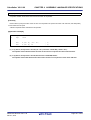
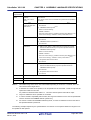
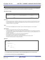
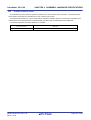
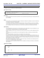
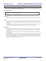
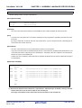
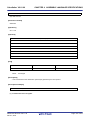
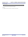
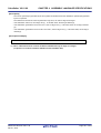
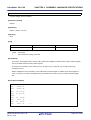
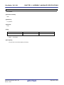
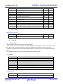
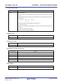
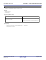
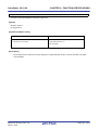
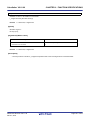
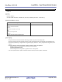
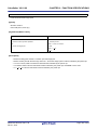
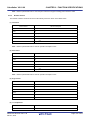
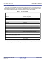
Notes 1.
When internal RAM area or SFR area is accessed or using the instruction for no data access.
2.
When program memory area is accessed.
3.
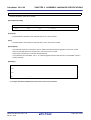
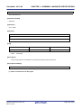
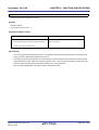
The flag field symbol shows the flag change at the time the instruction is executed.
Blank : Unchanged
0
: Cleared to 0
1
: Set to 1
x
: Set or cleared according to the result
R
: Previously saved value is restored
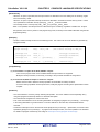
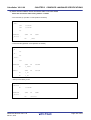
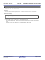
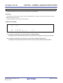
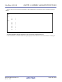
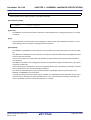
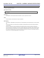
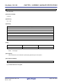
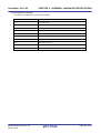
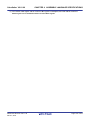
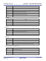
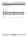
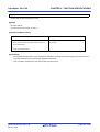
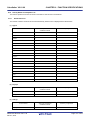
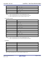
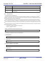
Remarks 1.
One clock of the instruction is one clock of the CPU clock (fCLK) that is selected by the processor clock
control register (PCC).
2.
Clock number when there is a program in the internal ROM (Flash memory) area.
3.
cnt is the number of bit shifts.
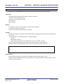
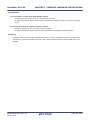
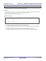
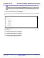
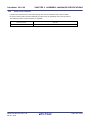
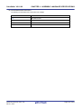
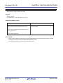
4.
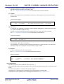
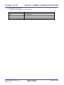
In products in which external memory area connects to internal flash area, when using external bus
interface function, wait number is added to the instruction execution clock number that is mapped to the
final address of Flash (maximum 16 bytes). This is because when carrying out a prior read of the
instruction code, flash space is exceeded and external memory space is accessed and so an external
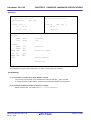
memory wait is entered. Please see "(b) Access to external memory contents as data" for wait numbers.
R20UT2774EJ0100 Rev.1.00
Dec 01, 2013
Page 454 of 872